ESST4B
Source: GridKit/Model/PhasorDynamics/Exciter/ESST4B/README.md
IEEE Type ST4B Potential- or Compound-Source Controlled-Rectifier Exciter Model (ESST4B)
ESST4B is a static excitation system with compensated-voltage sensing, an outer proportional/integral voltage regulator, a lag block, an inner proportional/integral regulator with exciter-output feedback, low-value over-excitation limiter gating, and potential- or compound-source rectifier scaling.
Notes:
Internal voltage and current signals are on model base unless otherwise stated.
The rectifier loading block \(F_{\mathrm{ex}}=f(I_N)\) is the source controlled-rectifier loading curve from Fig. 1; it is not a CommonMath helper.
The potential-source calculation uses explicit real and imaginary terminal voltage/current components; the diagram’s complex expression is not used as model-equation notation below.
Block Diagram
Standard model of the ESST4B Exciter.
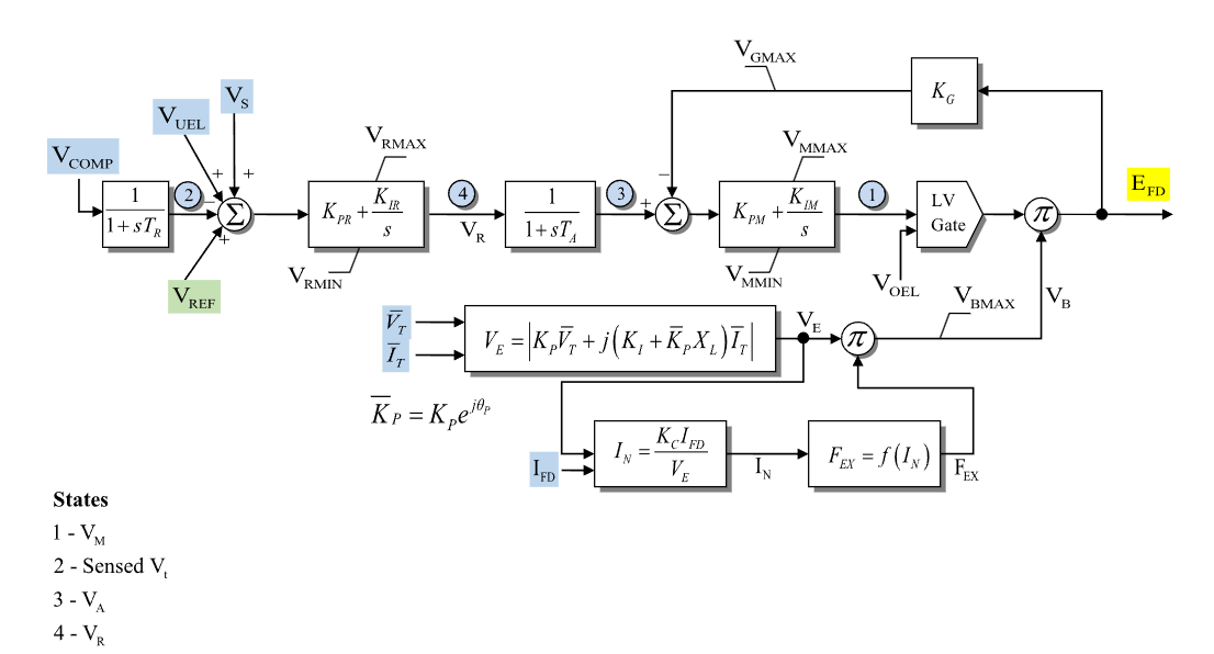
Figure 1: Exciter ESST4B model. Figure courtesy of PowerWorld
Model Parameters
Symbol |
Units |
JSON |
Description |
Typical Value |
Note |
|---|---|---|---|---|---|
\(T_R\) |
[sec] |
|
Compensated-voltage transducer time constant |
0.0 |
Block name: |
\(K_{\mathrm{pr}}\) |
[p.u.] |
|
Outer regulator proportional gain |
1.0 |
Block name: |
\(K_{\mathrm{ir}}\) |
[p.u./s] |
|
Outer regulator integral gain |
0.0 |
Block name: |
\(V_R^{\max}\) |
[p.u.] |
|
Maximum outer regulator output |
1.0 |
Block name: |
\(V_R^{\min}\) |
[p.u.] |
|
Minimum outer regulator output |
-1.0 |
Block name: |
\(T_A\) |
[sec] |
|
Regulator lag time constant |
0.0 |
Block name: |
\(K_{\mathrm{pm}}\) |
[p.u.] |
|
Inner regulator proportional gain |
1.0 |
Block name: |
\(K_{\mathrm{im}}\) |
[p.u./s] |
|
Inner regulator integral gain |
0.0 |
Block name: |
\(V_M^{\max}\) |
[p.u.] |
|
Maximum inner regulator output |
1.0 |
Block name: |
\(V_M^{\min}\) |
[p.u.] |
|
Minimum inner regulator output |
0.0 |
Block name: |
\(K_G\) |
[p.u.] |
|
Exciter-output feedback gain into inner regulator |
0.0 |
Block name: |
\(K_P\) |
[p.u.] |
|
Potential-source voltage coefficient magnitude |
0.0 |
Source label: |
\(K_I\) |
[p.u.] |
|
Potential-source current coefficient |
0.0 |
Source label: |
\(V_B^{\max}\) |
[p.u.] |
|
Maximum rectifier source multiplier |
999.0 |
Block name: |
\(K_C\) |
[p.u.] |
|
Rectifier loading current coefficient |
0.0 |
Block name: |
\(X_L\) |
[p.u.] |
|
Source reactance term in potential-source calculation |
0.0 |
Source label: |
\(\theta_P\) |
[deg] |
|
Potential-source coefficient angle |
0.0 |
Source label: |
\(V_G^{\max}\) |
[p.u.] |
|
Maximum exciter-output feedback signal |
999.0 |
Block name: |
Parameter Validation
Invalid ESST4B parameter sets are rejected by the following checks.
Model Derived Parameters
The potential-source coefficient is resolved into real scalar components:
Here \(\theta_P\) is converted from degrees before evaluating the trigonometric functions.
Model Variables
Internal Variables
Differential
Symbol |
Units |
Description |
Note |
|---|---|---|---|
\(V_M\) |
[p.u.] |
Inner regulator output |
State 1 in Fig. 1 |
\(V_C\) |
[p.u.] |
Sensed compensated voltage |
State 2 in Fig. 1; source label: |
\(V_A\) |
[p.u.] |
Lagged outer-regulator output |
State 3 in Fig. 1; algebraic when \(T_A=0\) |
\(x_R\) |
[p.u.] |
Outer regulator integral state |
State 4 in Fig. 1; source label: |
Algebraic
Symbol |
Units |
Description |
Note |
|---|---|---|---|
\(e_V\) |
[p.u.] |
Voltage-error signal into outer regulator |
Summing junction after sensed voltage |
\(V_R\) |
[p.u.] |
Limited outer regulator output |
Limited by \(V_R^{\min}\) and \(V_R^{\max}\) |
\(V_G\) |
[p.u.] |
Limited exciter-output feedback signal |
\(K_G E_{\mathrm{fd}}\) limited by \(V_G^{\max}\) |
\(e_M\) |
[p.u.] |
Inner regulator error |
\(V_A\) minus \(V_G\) |
\(V_{\mathrm{lv}}\) |
[p.u.] |
Low-value gate output |
Lesser of \(V_M\) and \(V_{\mathrm{oel}}\) |
\(V_{\mathrm{src}}^{\mathrm{r}}\) |
[p.u.] |
Real component of the potential-source expression |
From terminal voltage/current components |
\(V_{\mathrm{src}}^{\mathrm{i}}\) |
[p.u.] |
Imaginary component of the potential-source expression |
From terminal voltage/current components |
\(V_E\) |
[p.u.] |
Potential- or compound-source voltage magnitude |
Nonnegative source magnitude |
\(I_N\) |
[p.u.] |
Normalized exciter loading current |
Source label: |
\(F_{\mathrm{ex}}\) |
[p.u.] |
Rectifier loading factor |
Source label: |
\(V_B\) |
[p.u.] |
Rectifier source multiplier |
Limited by \(V_B^{\max}\) |
\(E_{\mathrm{fd}}\) |
[p.u.] |
Field-voltage output |
Product of low-value gate and \(V_B\) |
External Variables
Differential
None.
Algebraic
Symbol |
Units |
Description |
Note |
|---|---|---|---|
\(V_{\mathrm{comp}}\) |
[p.u.] |
Compensated voltage input |
Source label: |
\(V_{\mathrm{ref}}\) |
[p.u.] |
Voltage-control reference |
Source label: |
\(V_{\mathrm{uel}}\) |
[p.u.] |
Under-excitation limiter input |
Source label: |
\(V_S\) |
[p.u.] |
Stabilizer input signal |
Source label: |
\(V_{\mathrm{oel}}\) |
[p.u.] |
Over-excitation limiter input |
Source label: |
\(V_{\mathrm{r}}\) |
[p.u.] |
Terminal-voltage real component |
Source label: |
\(V_{\mathrm{i}}\) |
[p.u.] |
Terminal-voltage imaginary component |
Source label: |
\(I_{\mathrm{r}}\) |
[p.u.] |
Terminal-current real component |
Source label: |
\(I_{\mathrm{i}}\) |
[p.u.] |
Terminal-current imaginary component |
Source label: |
\(I_{\mathrm{fd}}\) |
[p.u.] |
Machine field current |
Source label: |
Model Equations
Differential Equations
CommonMath defines the Anti-Windup target and smooth approximation.
Algebraic Equations
CommonMath defines helper targets for min and clamp. The rectifier loading function \(f(I_N)\) is the source curve shown in Fig. 1.
Initialization
For a standard unsaturated start, the machine initializes \(E_{\mathrm{fd},0}\) and \(I_{\mathrm{fd},0}\) first. ESST4B reads those values, sets all internal derivatives to zero, and evaluates:
This closed-form start requires \(V_{E,0}\ne 0\), \(V_{B,0}\ne 0\), inactive \(V_R\), \(V_M\), \(V_G\), and \(V_B\) limits, and the low-value gate selecting \(V_M\). Starts with active low-value gate limiting or saturated PI states are outside these closed-form equations.
Model Outputs
Output |
Units |
Description |
Note |
|---|---|---|---|
|
[p.u.] |
Field-voltage output |
\(E_{\mathrm{fd}}\) |
|
[p.u.] |
Inner regulator output |
\(V_M\) |
|
[p.u.] |
Sensed compensated voltage |
\(V_C\) |
|
[p.u.] |
Lagged outer-regulator output |
\(V_A\) |
|
[p.u.] |
Outer regulator output |
\(V_R\) |
|
[p.u.] |
Exciter-output feedback signal |
\(V_G\) |
|
[p.u.] |
Low-value gate output |
\(V_{\mathrm{lv}}\) |
|
[p.u.] |
Potential-source voltage magnitude |
\(V_E\) |
|
[p.u.] |
Rectifier source multiplier |
\(V_B\) |
|
[p.u.] |
Normalized exciter loading current |
\(I_N\) |
|
[p.u.] |
Rectifier loading factor |
\(F_{\mathrm{ex}}\) |